Clas G Amplifier Circuit Diagram
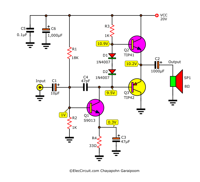
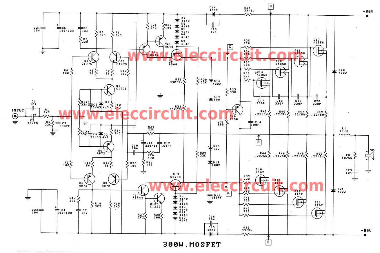
200 Watt Mosfet Amplifier Circuit To 300w On Class G
Class G Amplifiers
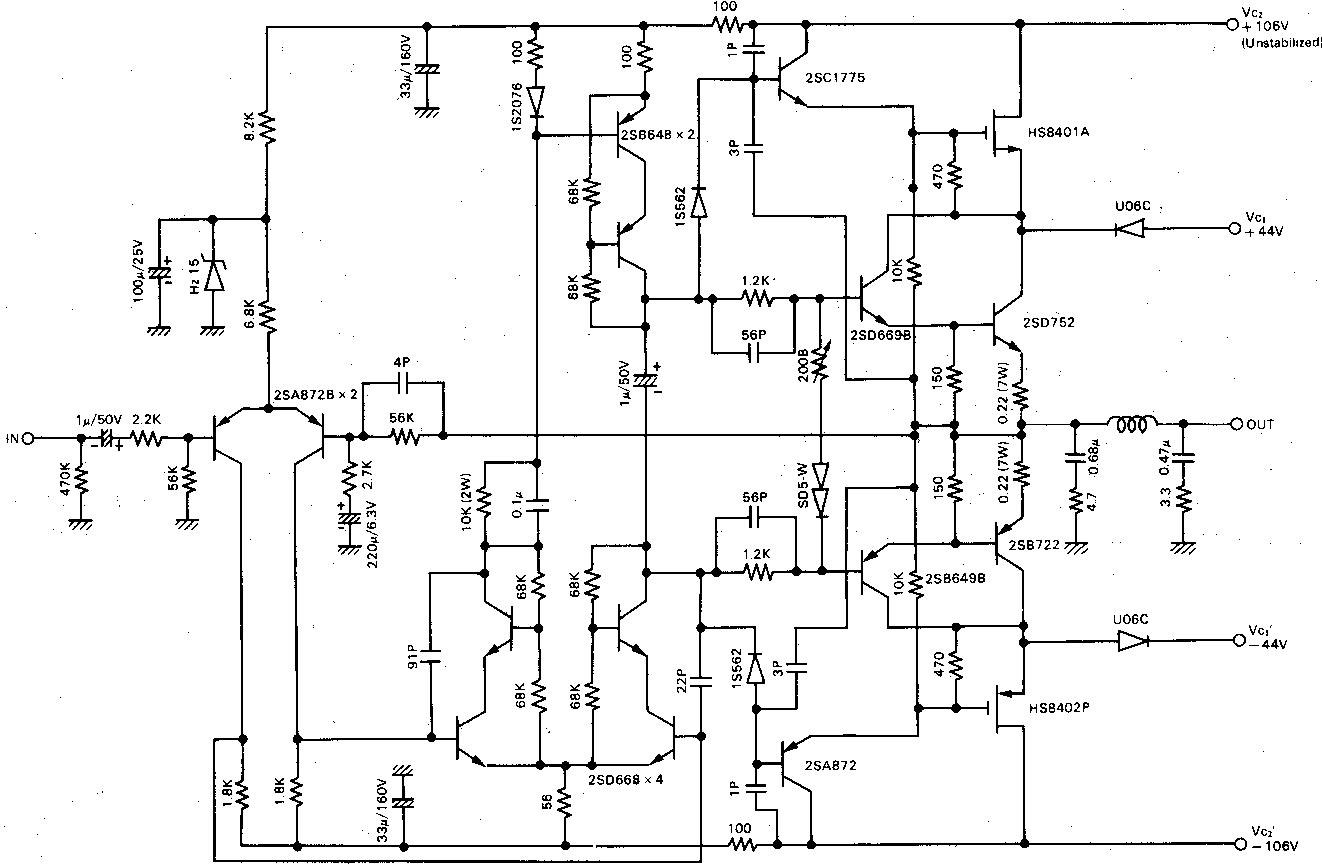
Figure 13 From Highest Efficiency And Super Quality Audio
Class d power amplifier is a type of audio amplifier were the power handling devices are operated as binary switches.
Clas g amplifier circuit diagram. Since the power handling devices mosfets works as perfect binary switches no time is wasted in between the transition of stages and no power is wasted in the zero input condition. A transistor biased in class ab mode produces an amplified output signal for only one half of the input signal. You can read more feature. The classes are based on the proportion of each input cycle conduction angle during which an amplifying device passes current.
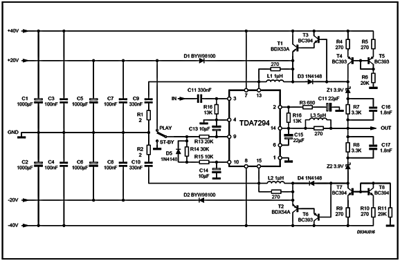
The main difference is that instead of ds. Which it is a high end for all your working. This is the 200 watt mosfet amplifier circuit on class g with pcb. Power amplifier circuits output stages are classified as a b ab and c for analog designsand class d and e for switching designs.
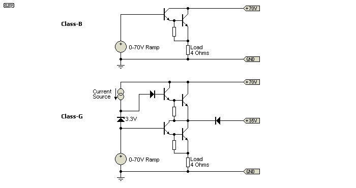
The image of the conduction angle derives from amplifying a sinusoidal signal. Audio amp circuit watt mosfet power amplifier circuit class g hybrid amplifier by andrea ciuffoli the audio research d also pioneer a and m use diamond buffer on output stage but these implement dynamic current generators. Figure 3 shows a similarly simplified schematic of a class g amp but using both polarities. Theory behind power amplifier circuit.
Class g h. A very common arrangement used in many commercial amps using class g is to operate the power transistors in series as shown in figure 2 note the drawing shows only one polarity and highly simplified. Linear mode power amplifiers class a b ab and class c are all linear mode amplifiers that have an output that is proportional to their input. 200 watts at load 8 ohms or 360 watts at the load 4 ohms.
Linear mode amplifiers do not saturate fully turn on or fully turn off. It is suitable for the pa system. Below you can see the block diagram of a basic pwm class d amplifier just like the one that we are building. It is based on the iraudamp1 reference design by international rectifier infineon.
How to build a class d power amp. The circuit diagram of the direct coupled class a power amplifier is shown in the figure below. Since the transistors in class a amplifier are forward biased all the time few current will flow through them even though there is no input signal and this is the main reason for its poor efficiency. An example of a class ab circuit left.
Below you can see the schematic of the amplifier that i designed. X watt quad audio amplifier here is the plete schematic diagram of one stereo course i used. Two important aspects of this circuit are class ab amplifiers and class a voltage amplifiers. Sourced from wikipedia and the emotiva xpa 1l class ab amplifier that operates in pure class a mode up to the first 35w right.
Since the transistors are always conducting heat is generated and continuously consuming power. Maximum rms output power.
The Classes And Classification Of Amplifiers And Its

Class G Amplifier With Two Supplies Download Scientific

200 Watt Mosfet Amplifier Circuit To 300w On Class G Audio
Class G Amplifiers

Max9730 2 4w Class G Power Amplifier
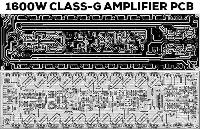
1600w Power Amplifier Class G Pcb Layout Electronic Circuit
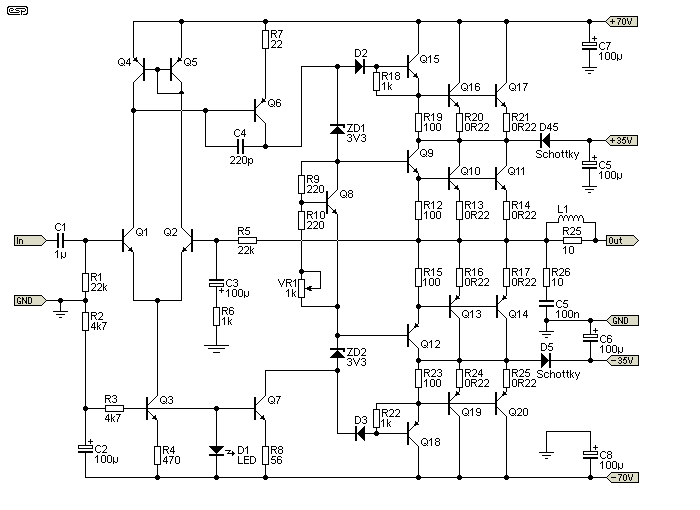
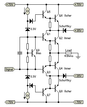
Class G Circlotrons

My Little Diy Class G Amplifier Blog Di Mauro Munzi

A Paul Kemble Web Page Audio Amplifier Protection

Amplifier Classes From A To H Circuit Cellar

The Signal Transfer Company Class G Amplifier

What Are Amplifier Classes And Their Power Efficiencies
300 1200w Mosfet Amplifier For Professionals Projects Circuits

Power Amplifier Classes Wikipedia
Class G Circlotrons

200 Watt Mosfet Amplifier Circuit To 300w On Class G E
200 Watt Mosfet Amplifier Circuit To 300w On Class G

Class A B D G H To T Audio Amplifiers
